Copyright (c) 2019 Journal of the Chilean Chemical Society

This work is licensed under a Creative Commons Attribution-NonCommercial-ShareAlike 4.0 International License.
Abstract
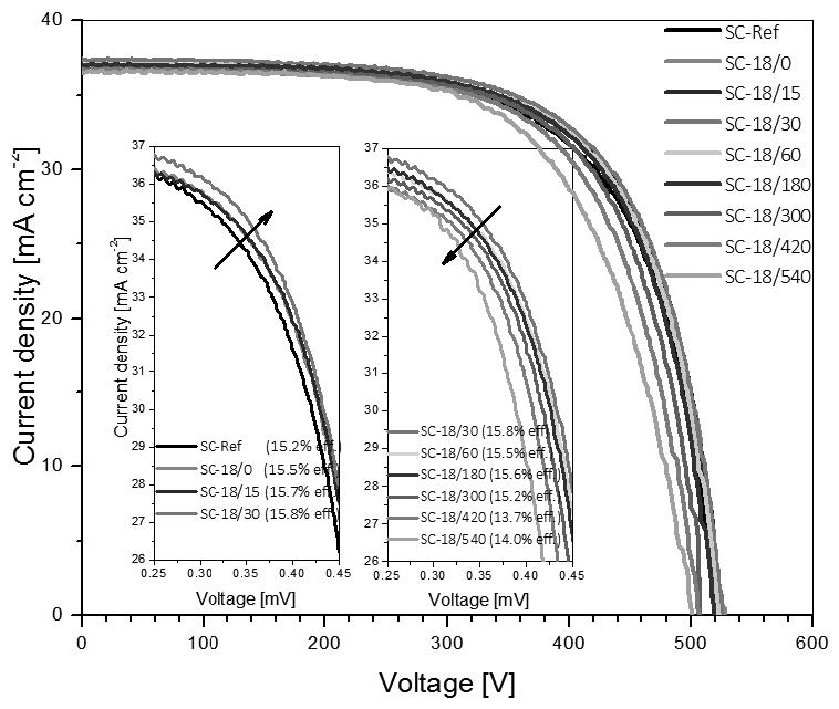
We present a simple method for the texturing of commercial silicon solar cells in a two-step process by etching in an HF solution containing H2O2. This etching process is facilitated by silver nanoparticles which act as catalytic sites. The etching times for the fabrication of nano-pores on the surface are established. The optical properties of the nano-structures on the surface of silicon solar cell were investigated by spectrometer measurements. The samples presented a total reflection coefficient lower than that of silicon solar cells without the treatment. The global efficiency of the silicon solar cell depends on the chosen preparation conditions for the silver ion concentration, and time of wet etching. The textured surface of solar cells showed an increase in efficiency, with a circuit photocurrent higher than that of a reference silicon solar cell without texturing. The J-V curves of various silicon cells are presented and discussed in correlation with the surface morphology.
References
- P. Spinelli, M.A. Verschuuren, and A. Polman, Nature Communications 3 (2012) 1.
- H. A. Macleod, Thin-film optical filters (American Elsevier Pub. Co., New York, 1969).
- J. de Boor, N. Geyer, J.V. Wittemann. U. Gosele, and V. Schmitdt, Nanotechnology 21, (2010). Y. Wu and P. Yang, J. Am. Chem. Soc. 123 (2001) 3165. S. Kodambaka, J. B. Hannon, R. M. Tromp, and F. M. Ross, Nano Lett. 6 (2006) 1292. T. Stelzner, M. Pietsch, G. Andrä, F. Falk, E. Ose and S. Christiansen, Nanotechnology 19 (2008) 1.
- a) D.S. Ruby, W.K. Scubert, J.M. Gee, and S.H. Zaidi, U.S. Patent No. 6091021, (2000). b) A. V. Whitney, B. D. Myers, and R. P. Van Duyne, Nano Lett. 4 (2004) 1507.
- H. D. Tong, H. V. Jansen, V. J. Gadgil, C. G. Bostan, E. Berenschot, C. J. van Rijn, and M. Elwenspoek, Nano Lett. 4 (2004) 283.
- a) J. Shao, E. A. Josephs, C. Lee, A. Lopez, and T. Ye, ACS Nano 7 (2013) 5421. b) A. Prasad, S. Balakrishnan, S. K. Jain, and G.C. Jain, Electrochem. Soc. 129 (1982) 596. c) T. Homma, H. Sato, K. Mori, T. Osaka, and S. Shoji, J. Phys. Chem. B 109 (2005) 5724.
- R. Torres, V. Vervisch, M. Halwax, T. Sarnet, P. Delaporte, M. Sentis, J. Ferreira, D. Barakel, S. Bastide, F. Torregrosa, H. Etienne, and L. Roux, Journal of Optoelectronics and Advanced Materials 12 (2010) 621.
- M. Bechelany, E. Berodier, X. Maeder, S. Schmitt, J. Michler, and L. Philippe, Appl. Mater. Interfaces 3 (2011) 3866.
- H. Han, Z. Huang, and W. Lee, Nanotoday 9 (2014) 271. H.C. Yuan, V. E. Yost, M. R. Page, L. Roybal, B. To, P. Stradins, D. L. Meier, and H. M. Branz, 34th IEEE Photovoltaic Specialists Conference, 141 (2009). R. Chaoui, B. Mahmoudi, and Y.S. Ahmed, Physica Status Solidi A 205 (2008) 1724.
- Y. Qu, L. Liao, Y. Li, H. Zhang, Y. Huang, and X. Duan, Nano Lett. 9 (2009) 4539.
- H. A. Atwater and A. Polman, Nat. Mater. 9 (2010) 205.
- X. Wang, J. Wang, and H. Wang, Solar Energy 101 (2014) 100.
- K.R. Catchpole and A. Polman, Opt. Express 16 (2008) 21723.
- X. Liu, P. R. Coxon, M. Peters, B. Hoex, J. M. Cole, and D. J. Fray, Energy Environ. Sci. 7 (2014) 3223.
- Y. Liu, G. Ji, J. Wang, X. Liang, Z. Zuo, and Yi Shi, Nanoscale Research Letters 7 (2012) 663.
- M. Algasinger, M. Bernt, S. Koynov, and M. Stutzmann, J. Appl. Phys. 115 (2014) 164308.
- S. Bastide, T. Nychyporuk, Z. Zhou, A. Fave, and M. Lemiti, Solar Energy Materials & Solar Cells 102 (2012) 26.
- Z. Huang, T.Shimizu, S. Senz, Z. Zhang, N. Geyer, and U. Gösele, J. Phys. Chem. C 114 (2010) 10683.
- K.Tsujino and M. Matsumura, Electrochimica Acta 53 (2007) 28.
- M. Lee and D. Khang, RSC Adv. 3 (2013) 26313.
- Joint Committee on Powder Diffraction Standars, silver file No. 04-0783.
- P.R. Pudasaini and A. Ayon, Microelectronic Engineering 110 (2013) 126.
- L. Zeng, X. Yu, Y. Han, and D. Yang, Journal of Nanomaterials 2012 (2012) 6.
- N. F. Fahim, B. Jia, Z. Shi, and M. Gu, Opt. Express 20 (2012) 694.
- J. Li, H. Y. Yu, Y. Li, F. Wang, M.Yang; and S. M. Wong, Appl. Phys. Lett. 98 (2011) 21905.
- Y. Liu, S.H. Sun, J. Xu, L. Zhao, H.C.Sun, L. Li, W.W.Mu, L. Xu, and K. J. Chen, Opt. Express 19 (2011) 1051.
- Z. Ouyang, S.Pillai, Fi.Beck, O. Kunz, S. Varlamov, K. R. Catchpole, P. Campbell, and M.A. Green, Applied physics letters 96 (2010) 261109.
- T. Yehua; Z. Chunlan ; W. Wenjing; Z. Su; Z. Yan; Z. Lei; L. Hailing; Y. Baojun; C. Jingwei, F. Jianming, and C. Hongbin, J. Semicond. 33 (2012) 064007.
- American Society for Testing and Materials, “ASTM G173 - 03 Standard Tables for Reference Solar Spectral Irradiances: Direct Normal and Hemispherical on 37° Tilted Surface,” 2012. [Online]. Available: https:// www.astm.org/Standards/G173.htm. [Accessed: 09-Sep-2016].
